1. Basic Residences and Nanoscale Behavior of Silicon at the Submicron Frontier
1.1 Quantum Confinement and Electronic Framework Makeover
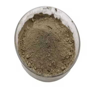
(Nano-Silicon Powder)
Nano-silicon powder, composed of silicon bits with characteristic dimensions listed below 100 nanometers, stands for a standard change from mass silicon in both physical behavior and functional energy.
While mass silicon is an indirect bandgap semiconductor with a bandgap of about 1.12 eV, nano-sizing generates quantum confinement results that fundamentally modify its electronic and optical residential or commercial properties.
When the bit size methods or falls below the exciton Bohr span of silicon (~ 5 nm), fee providers become spatially restricted, causing a widening of the bandgap and the introduction of noticeable photoluminescence– a sensation absent in macroscopic silicon.
This size-dependent tunability enables nano-silicon to release light throughout the visible spectrum, making it an appealing prospect for silicon-based optoelectronics, where traditional silicon stops working as a result of its poor radiative recombination performance.
Additionally, the boosted surface-to-volume proportion at the nanoscale boosts surface-related phenomena, consisting of chemical reactivity, catalytic task, and communication with electromagnetic fields.
These quantum impacts are not merely academic curiosities however form the structure for next-generation applications in energy, noticing, and biomedicine.
1.2 Morphological Variety and Surface Area Chemistry
Nano-silicon powder can be manufactured in various morphologies, including spherical nanoparticles, nanowires, permeable nanostructures, and crystalline quantum dots, each offering distinct advantages depending upon the target application.
Crystalline nano-silicon generally maintains the diamond cubic structure of mass silicon but displays a greater thickness of surface defects and dangling bonds, which must be passivated to support the product.
Surface area functionalization– usually attained via oxidation, hydrosilylation, or ligand attachment– plays an essential role in establishing colloidal security, dispersibility, and compatibility with matrices in compounds or organic environments.
For instance, hydrogen-terminated nano-silicon shows high sensitivity and is susceptible to oxidation in air, whereas alkyl- or polyethylene glycol (PEG)-covered fragments show enhanced stability and biocompatibility for biomedical use.
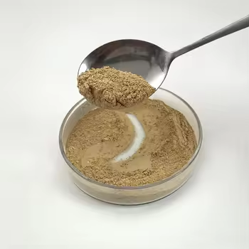
( Nano-Silicon Powder)
The visibility of an indigenous oxide layer (SiOₓ) on the bit surface, also in marginal amounts, considerably influences electric conductivity, lithium-ion diffusion kinetics, and interfacial responses, particularly in battery applications.
Understanding and controlling surface chemistry is as a result essential for harnessing the complete possibility of nano-silicon in practical systems.
2. Synthesis Approaches and Scalable Construction Techniques
2.1 Top-Down Techniques: Milling, Etching, and Laser Ablation
The production of nano-silicon powder can be generally classified right into top-down and bottom-up approaches, each with unique scalability, pureness, and morphological control qualities.
Top-down methods entail the physical or chemical decrease of bulk silicon right into nanoscale pieces.
High-energy sphere milling is a commonly made use of commercial method, where silicon pieces go through intense mechanical grinding in inert environments, leading to micron- to nano-sized powders.
While cost-efficient and scalable, this technique commonly presents crystal flaws, contamination from grating media, and broad particle dimension circulations, needing post-processing filtration.
Magnesiothermic reduction of silica (SiO ₂) complied with by acid leaching is an additional scalable course, especially when using natural or waste-derived silica sources such as rice husks or diatoms, offering a sustainable pathway to nano-silicon.
Laser ablation and reactive plasma etching are more precise top-down methods, capable of generating high-purity nano-silicon with controlled crystallinity, though at higher cost and reduced throughput.
2.2 Bottom-Up Approaches: Gas-Phase and Solution-Phase Growth
Bottom-up synthesis enables greater control over particle size, form, and crystallinity by developing nanostructures atom by atom.
Chemical vapor deposition (CVD) and plasma-enhanced CVD (PECVD) allow the growth of nano-silicon from aeriform forerunners such as silane (SiH ₄) or disilane (Si two H SIX), with parameters like temperature, stress, and gas flow determining nucleation and development kinetics.
These approaches are especially efficient for generating silicon nanocrystals embedded in dielectric matrices for optoelectronic gadgets.
Solution-phase synthesis, consisting of colloidal paths using organosilicon compounds, permits the manufacturing of monodisperse silicon quantum dots with tunable emission wavelengths.
Thermal decomposition of silane in high-boiling solvents or supercritical fluid synthesis also generates top notch nano-silicon with narrow dimension distributions, ideal for biomedical labeling and imaging.
While bottom-up methods usually produce remarkable material high quality, they face obstacles in massive manufacturing and cost-efficiency, necessitating recurring study right into crossbreed and continuous-flow procedures.
3. Energy Applications: Transforming Lithium-Ion and Beyond-Lithium Batteries
3.1 Role in High-Capacity Anodes for Lithium-Ion Batteries
Among the most transformative applications of nano-silicon powder hinges on energy storage, particularly as an anode material in lithium-ion batteries (LIBs).
Silicon offers a theoretical certain ability of ~ 3579 mAh/g based upon the formation of Li ₁₅ Si Four, which is nearly 10 times more than that of traditional graphite (372 mAh/g).
Nonetheless, the large quantity growth (~ 300%) during lithiation triggers bit pulverization, loss of electrical get in touch with, and continuous strong electrolyte interphase (SEI) development, bring about quick capability fade.
Nanostructuring reduces these issues by reducing lithium diffusion courses, fitting strain more effectively, and decreasing crack likelihood.
Nano-silicon in the kind of nanoparticles, permeable frameworks, or yolk-shell frameworks makes it possible for relatively easy to fix cycling with boosted Coulombic performance and cycle life.
Business battery technologies currently include nano-silicon blends (e.g., silicon-carbon compounds) in anodes to increase power thickness in customer electronics, electric vehicles, and grid storage systems.
3.2 Prospective in Sodium-Ion, Potassium-Ion, and Solid-State Batteries
Beyond lithium-ion systems, nano-silicon is being discovered in arising battery chemistries.
While silicon is less reactive with salt than lithium, nano-sizing enhances kinetics and allows minimal Na ⁺ insertion, making it a candidate for sodium-ion battery anodes, especially when alloyed or composited with tin or antimony.
In solid-state batteries, where mechanical security at electrode-electrolyte user interfaces is critical, nano-silicon’s capacity to undergo plastic deformation at little scales reduces interfacial anxiety and boosts get in touch with maintenance.
Additionally, its compatibility with sulfide- and oxide-based solid electrolytes opens up methods for safer, higher-energy-density storage options.
Study remains to maximize user interface engineering and prelithiation methods to make best use of the longevity and efficiency of nano-silicon-based electrodes.
4. Emerging Frontiers in Photonics, Biomedicine, and Composite Products
4.1 Applications in Optoelectronics and Quantum Source Of Light
The photoluminescent residential properties of nano-silicon have renewed efforts to develop silicon-based light-emitting tools, a long-standing difficulty in integrated photonics.
Unlike mass silicon, nano-silicon quantum dots can exhibit reliable, tunable photoluminescence in the visible to near-infrared array, making it possible for on-chip source of lights compatible with complementary metal-oxide-semiconductor (CMOS) innovation.
These nanomaterials are being integrated into light-emitting diodes (LEDs), photodetectors, and waveguide-coupled emitters for optical interconnects and picking up applications.
Furthermore, surface-engineered nano-silicon exhibits single-photon discharge under particular problem setups, positioning it as a prospective platform for quantum information processing and safe and secure interaction.
4.2 Biomedical and Environmental Applications
In biomedicine, nano-silicon powder is obtaining attention as a biocompatible, eco-friendly, and safe alternative to heavy-metal-based quantum dots for bioimaging and drug delivery.
Surface-functionalized nano-silicon bits can be developed to target certain cells, release therapeutic agents in feedback to pH or enzymes, and offer real-time fluorescence tracking.
Their degradation right into silicic acid (Si(OH)₄), a naturally taking place and excretable substance, reduces long-term toxicity issues.
In addition, nano-silicon is being checked out for ecological removal, such as photocatalytic destruction of toxins under visible light or as a lowering agent in water treatment processes.
In composite products, nano-silicon improves mechanical toughness, thermal stability, and wear resistance when incorporated right into metals, ceramics, or polymers, particularly in aerospace and auto elements.
Finally, nano-silicon powder stands at the junction of fundamental nanoscience and commercial advancement.
Its one-of-a-kind mix of quantum effects, high sensitivity, and flexibility across power, electronics, and life scientific researches underscores its role as a vital enabler of next-generation technologies.
As synthesis strategies development and combination difficulties are overcome, nano-silicon will certainly continue to drive progress towards higher-performance, sustainable, and multifunctional material systems.
5. Supplier
TRUNNANO is a supplier of Spherical Tungsten Powder with over 12 years of experience in nano-building energy conservation and nanotechnology development. It accepts payment via Credit Card, T/T, West Union and Paypal. Trunnano will ship the goods to customers overseas through FedEx, DHL, by air, or by sea. If you want to know more about Spherical Tungsten Powder, please feel free to contact us and send an inquiry(sales5@nanotrun.com).
Tags: Nano-Silicon Powder, Silicon Powder, Silicon
All articles and pictures are from the Internet. If there are any copyright issues, please contact us in time to delete.
Inquiry us