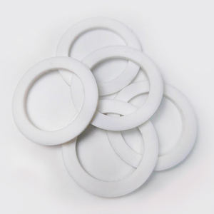
1. Product Basics and Structural Characteristics of Alumina Ceramics
1.1 Crystallographic and Compositional Basis of α-Alumina
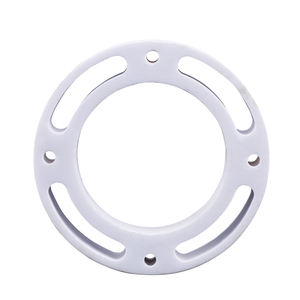
(Alumina Ceramic Substrates)
Alumina ceramic substratums, largely composed of light weight aluminum oxide (Al two O FOUR), work as the backbone of modern-day electronic packaging due to their extraordinary balance of electrical insulation, thermal stability, mechanical strength, and manufacturability.
The most thermodynamically secure stage of alumina at heats is corundum, or α-Al Two O SIX, which crystallizes in a hexagonal close-packed oxygen latticework with aluminum ions occupying two-thirds of the octahedral interstitial sites.
This dense atomic plan conveys high hardness (Mohs 9), superb wear resistance, and solid chemical inertness, making α-alumina ideal for rough operating settings.
Industrial substratums generally consist of 90– 99.8% Al Two O THREE, with small additions of silica (SiO TWO), magnesia (MgO), or rare earth oxides made use of as sintering aids to advertise densification and control grain growth throughout high-temperature handling.
Higher purity qualities (e.g., 99.5% and above) show premium electrical resistivity and thermal conductivity, while reduced pureness variations (90– 96%) provide affordable options for less requiring applications.
1.2 Microstructure and Problem Engineering for Electronic Reliability
The performance of alumina substrates in digital systems is seriously based on microstructural harmony and problem minimization.
A fine, equiaxed grain structure– typically varying from 1 to 10 micrometers– guarantees mechanical stability and minimizes the chance of crack propagation under thermal or mechanical tension.
Porosity, especially interconnected or surface-connected pores, must be minimized as it deteriorates both mechanical strength and dielectric performance.
Advanced processing methods such as tape casting, isostatic pressing, and controlled sintering in air or controlled ambiences make it possible for the production of substrates with near-theoretical thickness (> 99.5%) and surface area roughness below 0.5 µm, vital for thin-film metallization and cord bonding.
Additionally, contamination segregation at grain boundaries can cause leak currents or electrochemical migration under bias, demanding stringent control over resources pureness and sintering conditions to ensure long-term dependability in humid or high-voltage atmospheres.
2. Manufacturing Processes and Substratum Manufacture Technologies
( Alumina Ceramic Substrates)
2.1 Tape Casting and Green Body Handling
The manufacturing of alumina ceramic substrates begins with the preparation of an extremely spread slurry containing submicron Al ₂ O five powder, natural binders, plasticizers, dispersants, and solvents.
This slurry is processed using tape spreading– a continual method where the suspension is topped a moving service provider film making use of an accuracy doctor blade to accomplish uniform thickness, typically between 0.1 mm and 1.0 mm.
After solvent dissipation, the resulting “environment-friendly tape” is adaptable and can be punched, pierced, or laser-cut to form via openings for vertical interconnections.
Multiple layers might be laminated flooring to develop multilayer substratums for complex circuit assimilation, although most of industrial applications use single-layer configurations because of set you back and thermal development factors to consider.
The environment-friendly tapes are after that thoroughly debound to get rid of organic ingredients through managed thermal disintegration prior to last sintering.
2.2 Sintering and Metallization for Circuit Integration
Sintering is carried out in air at temperatures between 1550 ° C and 1650 ° C, where solid-state diffusion drives pore removal and grain coarsening to accomplish complete densification.
The linear contraction throughout sintering– commonly 15– 20%– have to be specifically forecasted and made up for in the style of eco-friendly tapes to ensure dimensional accuracy of the final substrate.
Following sintering, metallization is related to create conductive traces, pads, and vias.
2 key approaches dominate: thick-film printing and thin-film deposition.
In thick-film modern technology, pastes having steel powders (e.g., tungsten, molybdenum, or silver-palladium alloys) are screen-printed onto the substrate and co-fired in a minimizing atmosphere to develop robust, high-adhesion conductors.
For high-density or high-frequency applications, thin-film processes such as sputtering or dissipation are made use of to deposit bond layers (e.g., titanium or chromium) complied with by copper or gold, allowing sub-micron pattern via photolithography.
Vias are loaded with conductive pastes and terminated to develop electrical interconnections between layers in multilayer styles.
3. Useful Features and Performance Metrics in Electronic Systems
3.1 Thermal and Electric Actions Under Functional Stress
Alumina substrates are prized for their beneficial combination of modest thermal conductivity (20– 35 W/m · K for 96– 99.8% Al ₂ O TWO), which allows reliable warmth dissipation from power gadgets, and high quantity resistivity (> 10 ¹⁴ Ω · cm), making certain marginal leak current.
Their dielectric consistent (εᵣ ≈ 9– 10 at 1 MHz) is stable over a large temperature and frequency variety, making them suitable for high-frequency circuits approximately a number of ghzs, although lower-κ products like aluminum nitride are preferred for mm-wave applications.
The coefficient of thermal growth (CTE) of alumina (~ 6.8– 7.2 ppm/K) is reasonably well-matched to that of silicon (~ 3 ppm/K) and specific packaging alloys, decreasing thermo-mechanical stress and anxiety throughout gadget operation and thermal biking.
However, the CTE inequality with silicon stays an issue in flip-chip and direct die-attach setups, typically calling for certified interposers or underfill materials to minimize exhaustion failing.
3.2 Mechanical Robustness and Environmental Toughness
Mechanically, alumina substrates show high flexural strength (300– 400 MPa) and excellent dimensional stability under load, allowing their use in ruggedized electronics for aerospace, automotive, and industrial control systems.
They are resistant to resonance, shock, and creep at raised temperatures, preserving architectural integrity as much as 1500 ° C in inert atmospheres.
In damp settings, high-purity alumina shows minimal wetness absorption and superb resistance to ion movement, guaranteeing long-lasting integrity in outside and high-humidity applications.
Surface area solidity likewise safeguards against mechanical damages throughout handling and assembly, although care must be required to stay clear of edge breaking as a result of inherent brittleness.
4. Industrial Applications and Technical Effect Across Sectors
4.1 Power Electronics, RF Modules, and Automotive Solutions
Alumina ceramic substratums are common in power digital modules, including protected gate bipolar transistors (IGBTs), MOSFETs, and rectifiers, where they supply electrical isolation while promoting heat transfer to warmth sinks.
In radio frequency (RF) and microwave circuits, they work as service provider systems for crossbreed integrated circuits (HICs), surface acoustic wave (SAW) filters, and antenna feed networks because of their secure dielectric buildings and reduced loss tangent.
In the automobile industry, alumina substratums are utilized in engine control systems (ECUs), sensor packages, and electrical automobile (EV) power converters, where they withstand heats, thermal cycling, and exposure to harsh fluids.
Their integrity under harsh conditions makes them vital for safety-critical systems such as anti-lock braking (ABS) and advanced chauffeur aid systems (ADAS).
4.2 Clinical Instruments, Aerospace, and Emerging Micro-Electro-Mechanical Equipments
Beyond customer and industrial electronics, alumina substrates are employed in implantable clinical devices such as pacemakers and neurostimulators, where hermetic sealing and biocompatibility are extremely important.
In aerospace and defense, they are used in avionics, radar systems, and satellite communication components because of their radiation resistance and stability in vacuum environments.
Moreover, alumina is increasingly made use of as an architectural and shielding system in micro-electro-mechanical systems (MEMS), including pressure sensors, accelerometers, and microfluidic gadgets, where its chemical inertness and compatibility with thin-film processing are useful.
As digital systems continue to require greater power densities, miniaturization, and reliability under severe problems, alumina ceramic substrates continue to be a foundation product, bridging the void between efficiency, expense, and manufacturability in sophisticated digital packaging.
5. Distributor
Alumina Technology Co., Ltd focus on the research and development, production and sales of aluminum oxide powder, aluminum oxide products, aluminum oxide crucible, etc., serving the electronics, ceramics, chemical and other industries. Since its establishment in 2005, the company has been committed to providing customers with the best products and services. If you are looking for high quality alumina toughened zirconia, please feel free to contact us. (nanotrun@yahoo.com)
Tags: Alumina Ceramic Substrates, Alumina Ceramics, alumina
All articles and pictures are from the Internet. If there are any copyright issues, please contact us in time to delete.
Inquiry us